2022
 Nano-HySiF project Nano-HySiF project |
|
 Wafer with AI chips Wafer with AI chips |
|
 Springer Theses Prize Springer Theses Prize |
|
 |
|
 SensIC project SensIC project |
|
 PhotonQ project PhotonQ project |
|
2023
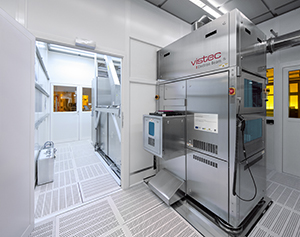 Vistec E-Beam SB255 |
|
 |
|
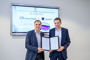 Prof. Dr. Joachim Burghartz and Michael Förtsch, Managing Director of Q.ANT |
|
 |
|
 © Kuzmick – stock.adobe |
|
2020
 |
|
 The Minister of Commerce, Dr. Nicole Hoffmeister-Kraut, delivers the authorization for the “BW CPS” project
 |
|
 Multi-Elektrode Chip
 |
|
 |
|
 |
|
 Concept for optical particle measurement Concept for optical particle measurement |
|
2021
 MikroSystemTechnik Kongress 2021
 |
|
 |
|
 First Place Best Paper Award
 |
|
 |
|
 |
|
 |
|
2018
 Coverstory in IEEE Journal
 |
|
 |
|
 ParsiFAl 4.0 project
 |
|
|
|
 |
|
 |
|
2019
 EUV stepper system with sketched beam path of the EUV light EUV stepper system with sketched beam path of the EUV light |
|
 Wafer with Si energy filter membranes
 |
|
 |
|
 Fully automated standard measurements of high-performance electronics
 |
|
 |
|
 Dürr Supplier Award ceremony
 |
|
2016
 Lithium-ion cells with embedded system to monitor functions
 |
|
 Photonic chip with echelle grating for fast optical data communication
 |
|
 |
|
 |
|
 Minister of Economic Affairs Dr. Nicole Hoffmeister-Kraut handed over a funding notification
 |
|
2017
|
|
 TENECOR EEG chip
 |
|
|
|
 |
|
 6” GaN on silicon and 2” bulk GaN wafer
 |
|
 innBW institute
|
|
2014
 FlexPacFAM – flexible packaging
 |
|
 Photo diode ASIC placed on laser diode Photo diode ASIC placed on laser diode |
|
 Intelligent Service Robotic through 3D imaging and processing
 |
|
 Self-adapting intelligent multi-aperture camera module
 |
|
 Granting of the J. J. Ebers Award
 |
|
2015
 VPG400 laser direct writer from Heidelberg Instruments
 |
|
 Foil-based silicon needles Foil-based silicon needles |
|
 MEMS – DMFC fuel cell
 |
|
 Loading the etcher with a DOE blank Loading the etcher with a DOE blank |
|
 Finalizing MicroTEC Südwest Spitzencluster
 |
|
2012
 CATRENE Innovation Award
 |
|
 |
|
 Demonstration Award
 |
|
 |
|
 |
|
2013
 KoSiF “complex systems in foil”
 |
|
 |
|
 Opening ceremony of the clean room expansion
 |
|
 Photonic integration
 |
|
 IEEE EDS PhD Fellowship Award 2013
 |
|
20009
 Gaussian Shape Beam by NIL Techno
 |
|
 Jack Raper Award
 |
|
 Hyperbraille Display
 |
|
2010
 REM image of an electron beam deflection unit for the “CHARPAN” project
 |
|
 |
|
 |
|
 TanDEM-X – radar satellite
 |
|
2011
 Cleanroom ground breaking ceremony
 |
|
 innBW Innovation Alliance Baden-Württemberg
 |
|
 |
|
 First PRONTO workshop
 |
|
 GMM-Preis 2011
 |
|
2007
 SafetyEYE® camera system |
|
| |
 REM image of a template with 60 nm pillars for the “FANTASTIC” project |
|
| |
 Ultra-thin microchip: 20 µm thickness |
|
 |
|
2008
 Webseite VIP |
|
Radar satellite TerraSAR-X |
|
 IdeenPark 2008 in Stuttgart |
|
 Festive ceremony at Haus der Wirtschaft in Stuttgart |
|
 Ultra-thin RFID chip on foil substrate |
|
 |
|
2004
 Cantilever Array
 |
|
|
2005
 EUV full field masks
 |
|
 |
|
 Joachim Burghartz
 |
|
 Image sensor chip IVP
 |
|
|
2006
 |
|
 Chipfilm
 |
|
|
2001
 IC_Lab experimental board
 |
|
 Klaus von Klitzing
 |
|
 ZBA350
 |
|
|
2002
 APS star sensor camera
 |
|
|
|
|
|
|
|
|
|
 10000 pixel – line sensor
 |
|
2003
 |
|
 Photomask Best Paper Award
 |
|
|
|
 HIPSCAN System
 |
|
1998
 MORE-Phone |
|
 Aircraft docking system |
|
 SIOP SIOP neuro processor chip |
|
1999
 Retina implant |
|
 SOI membrane mask |
|
 Recording using HDRC® camera |
|
 FeLS start screen |
|
2000
 Low-Power Design Award |
|
|
|
 T-Gate (REM image) |
|
 Circular line sensor |
|
|
1995
 Single chip controller |
|
 CECC EN 100114 part 1 certification |
|
 EDA award |
|
|
1996
 |
|
 VISION prize 1996 |
|
 EASIE model trial |
|
|
1997
 Loglux camera |
|
 1. Photo diode array for subretinal implants |
|
|
|
|
|
|
1992
SMC group picture |
|
 Basic patent HDRC®-Bildsensoren |
|

1993
 3D Chip |
|
 ISO 9001 certification |
|
|
|
|
1994
 Bosch radio equipment with IMS HF transistors |
|
 Vector Arithmetic Coprocessor |
|
 SAND Board |
|
1989
2-µm-GATE FOREST |
|
|
|
|

1990
COMETT course participants |
|
Test structure layout |
|
MCM on Si carrier |
|


1991
AMK ASIC „AC3“ |
|
Wafer bonding |
|
6 inch wafer |
|


1986
Inauguration ceremony |
|
Clean room |
|


1987
Hohner chip |
|
|
|
|

1988
HL700 e-beam writer |
|
Control chip for fluorescent displays |
|
„Multi-Projekt-Chip“ |
|


1983
 |
|
|
1984
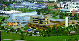
IMS facility |
|
1985
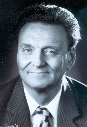
Prof. Dr. Bernd Höfflinger |
|
|
|
|